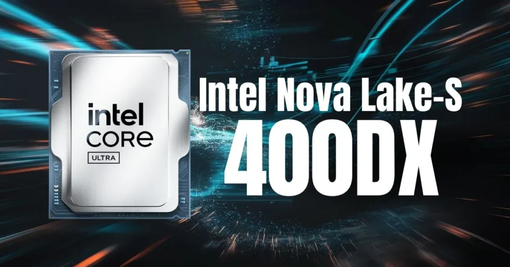
Intel Nova Lake-S Cache Map Revealed: 52-Core Flagship Packs 288MB
The specifications for Intel’s next-generation desktop platform, Nova Lake-S, are coming into sharper focus. Following last week’s leak of the preliminary SKU list (6 to 52 cores, DDR5-8000, forward socket compatibility), leaker Jaykihn has now shared the missing piece: detailed cache totals for the Core Ultra 400D and 400DX class parts.
The new information fills in the bLLC (Big Last Level Cache) figures across the lineup, showing exactly how Intel plans to differentiate its high-end desktop (HEDT) and mainstream models.
Cache Totals by Core Configuration
According to the leak, the cache hierarchy scales directly with core counts and die complexity:
- 52 cores (16+32+4 LP-E): 288MB bLLC – This is the top dual‑tile flagship, likely branded as Core Ultra 400DX. It targets the 175W TDP HEDT segment.
- 44 cores (16+24+4 LP-E): 264MB bLLC – The second dual‑tile SKU, also a 175W part, now confirmed with its own distinct cache figure.
- 28 cores (8+16+4 LP-E): 144MB bLLC – The highest single‑tile mainstream part, expected as Core Ultra 9 400D at 125W.
- 24 cores (8+12+4 LP-E): 132MB bLLC – A Core Ultra 7 400D variant at 125W.
- 22 cores (6+12+4 LP-E): 108MB bLLC – A lower‑tier Core Ultra 9 (non‑D) at 65W.
These totals align with earlier reports that Intel is using a cluster‑based cache layout. Jaykihn describes the bLLC arrangement as “4(2×12) + 312″ – meaning each P‑core cluster carries two 12MB slices, while each E‑core cluster carries one 12MB slice. That architecture explains how the 52‑core design reaches 288MB (12 slices × 24MB equivalent).
What This Means for Intel’s Stack
The new data clarifies a previously vague part of the Nova Lake-S roadmap. Earlier leaks mentioned “up to 288MB” cache but didn’t break down how that figure applied to different SKUs. Now we have distinct numbers for the dual‑tile parts (288MB and 264MB) and the single‑tile big‑cache models (144MB and 132MB). The 108MB entry appears on a 22‑core part without the “D” or “DX” suffix, suggesting it may lack the full bLLC implementation.
The 400D and 400DX branding likely denotes the presence of the larger cache stacks. The “DX” suffix may be reserved for the top dual‑tile HEDT chips, while “D” applies to single‑tile high‑cache mainstream models. Intel has not officially confirmed this naming.
Competitive Context
With AMD’s 3D V‑Cache technology already offering 96MB to 192MB on Ryzen 9000 X3D parts (and the 9950X3D2 reaching 208MB total cache), Intel’s bLLC approach appears aimed at matching or exceeding those figures. The 288MB flagship would be the largest cache ever seen on a consumer x86 desktop processor, potentially giving Intel a significant edge in cache‑sensitive gaming and productivity workloads.
Thanks. Had to delete my previous post because my math didn't quite math lol
— three twenty six (@326powah) April 18, 2026
Seems like L3 slices topology still correlates to amount of P-cores + E-clusters, not P-clusters + E-clusters? Since 132 is only possible with 11x12MB?
However, much depends on latency, architecture efficiency, and real‑world software support. The bLLC is integrated into the compute tile rather than stacked vertically (unlike AMD’s 3D V‑Cache), which may affect performance characteristics.
Also, Read
- AMD Ryzen 9 9950X3D2 Hits Amazon for $999 Pre-Order—$100 Above Official MSRP
- Ryzen 9 9950X3D2 Benchmarks Surface on HWBOT: Air-Cooled, 220W, Launching April 22
- Intel Core Ultra 400 “Nova Lake-S” Preliminary SKU List Leaks: 6 to 52 Cores, DDR5-8000, Forward Socket Compatibility
Looking Ahead
Nova Lake‑S is expected to enter mass production in Q4 2026, with a desktop launch likely at CES 2027 (January). The platform uses the new LGA‑1954 socket and 900‑series chipsets, and Intel has explicitly promised forward socket compatibility for the first time.
For enthusiasts, the cache leak confirms that Intel is taking cache capacity seriously. The 288MB figure is a statement of intent – whether it translates into a performance crown remains to be seen.
Source: Jaykihn